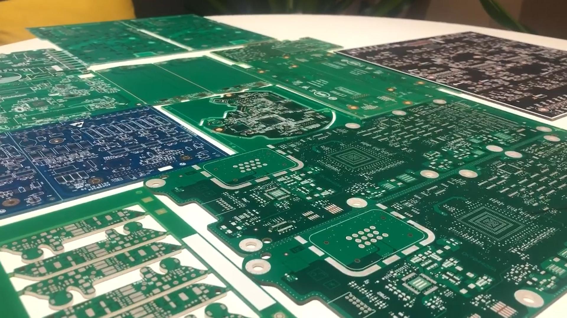
This is a general guide to the best practice printed circuit board (PCB) design rules for a high frequency or radio frequency (RF) circuit. Following these rules will help you to avoid some of the most common pitfalls in RF design. Poor PCB layout is one of the most common causes of inadequate transmit or receive performance and EMC failures due to spurious emissions. Ideally an engineer undertaking a PCB design should be familiar with the IPC standards as these provide a rich source of information and best practice on the general principles of PCB design.
When planning to layout an RF PCB, the first place to start is to contact your preferred board manufacturer and obtain a set of their guidelines and manufacturing capabilities. Click here on high frequency pcb to get more info about our site.
This will include the minimum track and gap widths, drill sizes and other key parameters. The board manufacturer should also be able to provide you with their standard layer stack and material data, this will include the copper weights, dielectric constant, and the thickness of core and pre-preg layers in multi-layer boards. Unless your circuit is extremely simple I suggest that a 4 layer board is used this ensures a continuous ground plane. When using a double sided board it is very difficult to ensure that the ground plane is un-broken. Another advantage of a 4 layer board is that the dimensions of the micro-strip for a 50 or 75 ohm design are more manageable. Use a micro-strip calculator to determine the required track width for the design impedance and ensure that it is within the manufactures capabilities, if not you may need to discuss the layer-stack with the manufacturer and select a non-standard build.
Another point to note is that in my experience attempting to maintain separate ground nets for different signal area's usually causes problems rather than any benefit and is largely a throwback to the days prior to multilayer boards, a single low impedance ground plane is the safest route.
It is quite acceptable to use FR4 for boards up-to 2.4GHz unless the highest level of performance is required. In certain circumstances it is worth specifying the board as controlled impedance to provide consistent RF performance.
Having determined the track and board geometries the next step is to address the component placement. Ensure that the RF components are laid out such that all the RF tracks can be kept on the top surface with minimum length and changes of direction. Start with low signal level areas at the antenna or RF input and work backwards towards the baseband or digital area. Keep digital and power supply areas away from the analogue RF circuitry and keep all the RF components on one side of the board.
Where your RF tracks can't be run in a straight line, use mitered bends if your CAD system supports them, never use right angled bends on RF signal lines. If mitered bends are not supported use a series of 45 degree bends or arcs, this minimizes impedance mismatches which would increase losses and spurious emissions.
On RF layouts it is common to provide a ground flood on the top layer and to "stitch" this to the ground plane by using multiple via's. If you intend to do this, ensure that the copper is kept a suitable distance from the RF tracks and components otherwise the impedance will be lowered and cause more harm than good. The via spacing can be 5-10mm apart there is very little benefit in stitching via's being closer than 5mm apart.
